
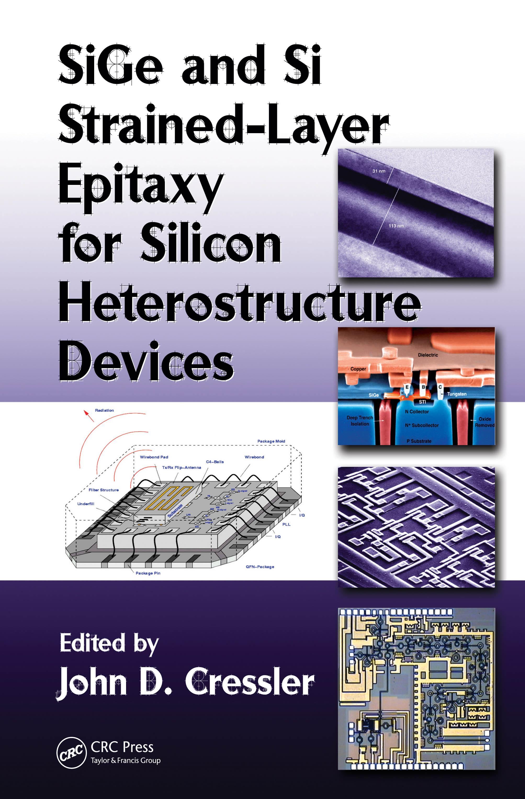
What seems routine today was not always so. The field of Si-based heterostructures rests solidly on the shoulders of materials scientists and crystal growers, those purveyors of the semiconductor “black arts” associated with the deposition of pristine films of nanoscale dimensionality onto enormous Si wafers with near infinite precision. We can now grow near-defect free, nanoscale films of Si and SiGe strained-layer epitaxy compatible with conventional high-volume silicon integrated circuit manufacturing. SiGe and Si Strained-Layer Epitaxy for Silicon Heterostructure Devices tells the materials side of the story and details the many advances in the Si-SiGe strained-layer epitaxy for device applications.
Drawn from the comprehensive and well-reviewed Silicon Heterostructure Handbook, this volume defines and details the many advances in the Si/SiGe strained-layer epitaxy for device applications. Mining the talents of an international panel of experts, the book covers modern SiGe epitaxial growth techniques, epi defects and dopant diffusion in thin films, stability constraints, and electronic properties of SiGe, strained Si, and Si-C alloys. It includes appendices on topics such as the properties of Si and Ge, the generalized Moll-Ross relations, integral charge-control relations, and sample SiGe HBT compact model parameters.
Pay easily by card, Klarna, Apple Pay or Google Pay. Not happy? You always have a 14-day money-back guarantee. Read more in our terms. If you have any questions, email us at hello@memmo.org.
Memmo makes studying easier – wherever you are in the world. We bring your course books and smart study tools together in one place: summaries, quizzes, podcasts and flashcards. Plus Ted, your study buddy who answers anything you wonder. Over 50,000 students already study here – built to help you learn faster and stress less.