
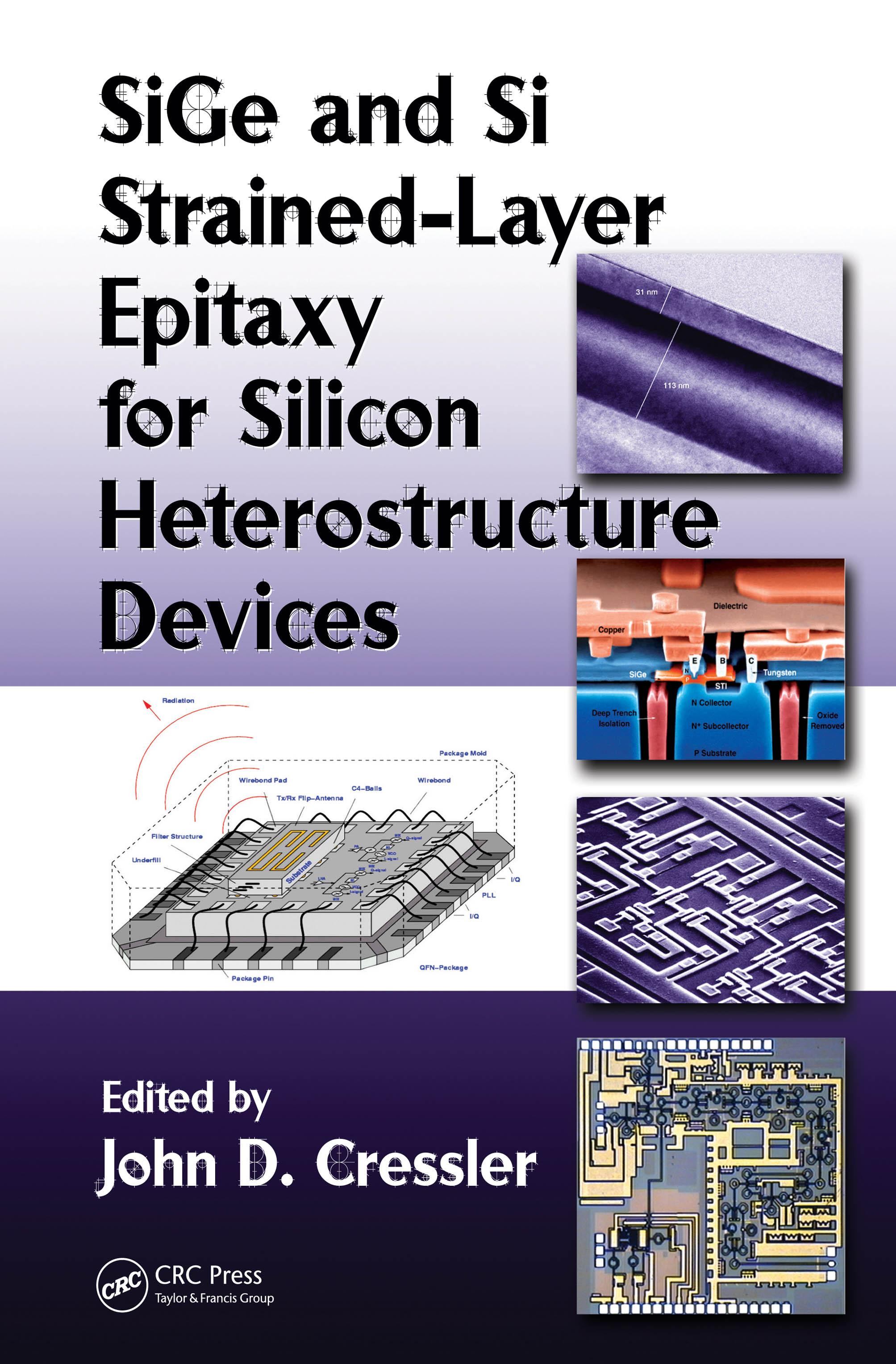
What seems routine today was not always so. The field of Si-based heterostructures rests solidly on the shoulders of materials scientists and crystal growers, those purveyors of the semiconductor “black arts” associated with the deposition of pristine films of nanoscale dimensionality onto enormous Si wafers with near infinite precision. We can now grow near-defect free, nanoscale films of Si and SiGe strained-layer epitaxy compatible with conventional high-volume silicon integrated circuit manufacturing. SiGe and Si Strained-Layer Epitaxy for Silicon Heterostructure Devices tells the materials side of the story and details the many advances in the Si-SiGe strained-layer epitaxy for device applications.
Drawn from the comprehensive and well-reviewed Silicon Heterostructure Handbook, this volume defines and details the many advances in the Si/SiGe strained-layer epitaxy for device applications. Mining the talents of an international panel of experts, the book covers modern SiGe epitaxial growth techniques, epi defects and dopant diffusion in thin films, stability constraints, and electronic properties of SiGe, strained Si, and Si-C alloys. It includes appendices on topics such as the properties of Si and Ge, the generalized Moll-Ross relations, integral charge-control relations, and sample SiGe HBT compact model parameters.
Płać wygodnie kartą, Klarną, Apple Pay lub Google Pay. Nie jesteś zadowolony? Zawsze masz 14-dniową gwarancję zwrotu pieniędzy. Więcej przeczytasz w naszych warunkach. Masz pytania? Napisz do nas na hello@memmo.org.
Memmo ułatwia naukę – gdziekolwiek jesteś na świecie. U nas znajdziesz podręczniki i sprytne narzędzia do nauki w jednym miejscu: streszczenia, quizy, podcasty i fiszki. A do tego Ted, Twój kumpel do nauki, który odpowie na wszystko, co Cię nurtuje. Ponad 50 000 studentów już tu się uczy – stworzone, byś uczył się szybciej i mniej stresował.